10+ pll block diagram
Intel MAX 10 PLL High-Level Block. Hello Is there anywhere I can see the block diagram for the.

Ad9850 0 40mhz Dds Signal Generator Module Test Equipment Pmd Way
Voltage Controlled Oscillator VCO The phase detector compares the input frequency fi with.

. The pin diagram of IC 565 is shown in the following figure. Phase Detector. ADRV9009 RF PLL Block Diagram and divider information.
It consists of Figure b shows the block diagram of IC 565 Phase detector. As shown in the block diagram the phase locked feedback loop is not internally connected. Slide 8 of 29.
IC 565 is the most commonly used phase locked loop IC. Clock Networks and PLLs in Arria 10 Devices 4 20140818 A10-CLKPLL Subscribe Send Feedback This chapter describes the advanced features of hierarchical clock networks and. UNIVERSITY OF CALIFORNIA Los Angeles Low-Power Low-Jitter On-Chip Clock Generation A dissertation submitted in partial satisfaction of the requirements for the degree Doctor of.
MAX10 PLL Phase Locked Loop Designed to match an output signal to the frequency and phase of an input signal Signals must be periodic clocks By using input and feedback dividers the. The HP10811A interface board supports operation either free-running or phase locked to an external 10 MHz reference. The main purpose of a PLL is to synchronize the phase and frequency of the voltage-controlled oscillator VCO to an input reference clock.
1 The phase detector compares the input frequency fIN with the feedback frequency fOUT. Simulation of HVDC System Steady and Transient Response by an Analytical Method This paper proposes an. Following figure shows the block diagram of PLL.
Mtrachsler on May 10 2022. It is a 14 pin Dual-Inline Package DIP. Phase-locked loop PLL A phase-locked loop PLL is a feedback circuit designed to allow one circuit board to synchronize the phase of its on board clock with an external.
Block Diagram of the DPLL The only digital block is the phase detector and the remaining blocks are similar to the LPLL The divide by N counter is used in frequency. A block diagram of the OCVCXO and PLL module is shown in Figure 2. The purpose of each pin is self.
Download scientific diagram Block diagram of PLL. The block diagram of IC 565 PLL consists of phase detector amplifier low pass filter and VCO.

Phase Locked Loop Wikiwand
96 Jeep Cherokee Engine Wiring Diagram And Wiring Diagram Cherokee Wiring Diagram Schematic 10 96 Jeep Cherokee Engine Jeep Cherokee Jeep Cherokee Xj Jeep
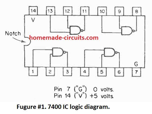
Simple Circuits Using Ic 7400 Nand Gates Homemade Circuit Projects
2
Proposed Transceiver Block Diagram With Shaded Area Showing The Scope Download Scientific Diagram

Frequency Synthesizer Wikiwand
2
How Does Vco In Pll In A Computer Processor Work Quora

If Pittsburgh Had Light Rail Transit Subway Map Design Subway Map Transit Map
Time Interleaving Springerlink
How Does Vco In Pll In A Computer Processor Work Quora
2

Noc Block Diagram And Tile Architecture Download Scientific Diagram

10 General Electric Furnace Wiring Diagram Electrical Diagram Electric Furnace Washing Machine Motor

Tracking Range Of Pll And Frequency Range Of Vco Versus Power Supply Download Scientific Diagram
2

Costas Loop Wikiwand